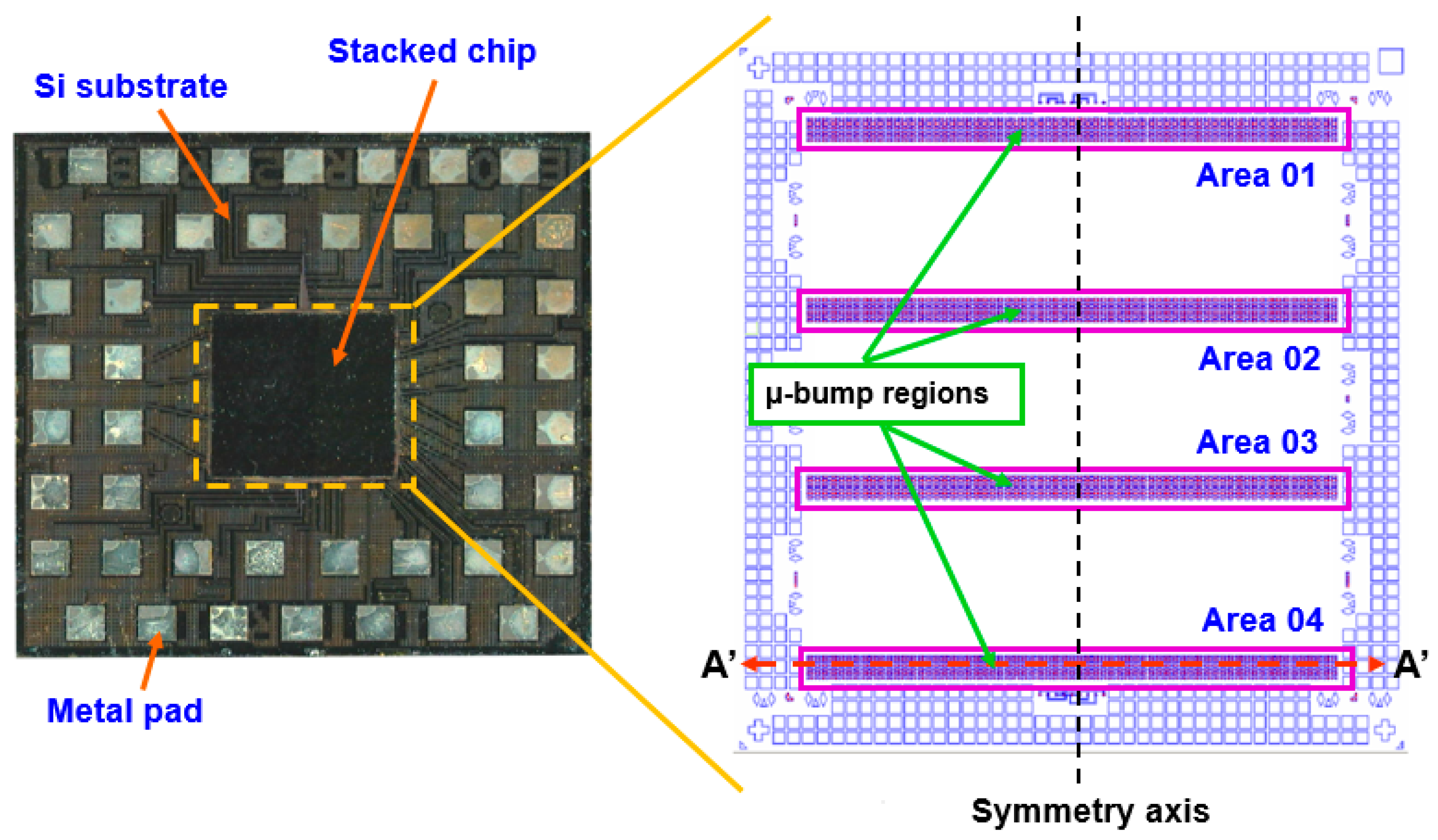
Details of test chip designs: pad pitch, layout, materials, and

Chip scale package basics, Advanced PCB Design Blog

David WHALLEY, Visiting Fellow, B.Sc. M.Phil.

Introduction of Plastic Ball Grid Array (PBGA) - FS PCBA

Electronics, Free Full-Text

Changqing LIU, Loughborough University, Loughborough

High-performance, power-efficient three-dimensional system-in-package designs with universal chiplet interconnect express
Materials, Free Full-Text

AN-772: A Design and Manufacturing Guide for the Lead Frame Chip Scale Package (LFCSP)

How To Design A BGA, PDF, Printed Circuit Board
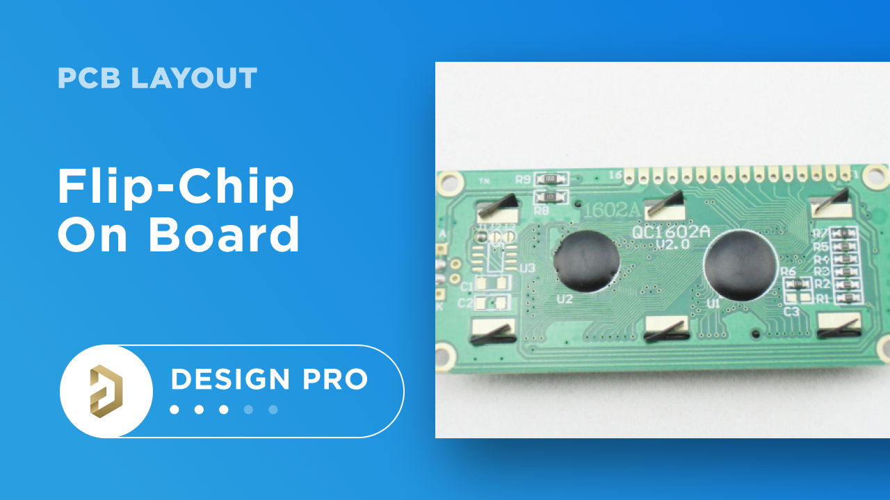
PCB Design Rules for Chip-on-Board Layout

Taking on the 0.3 mm ultra-fine pitch device challenge in PCB design

David WHALLEY, Visiting Fellow, B.Sc. M.Phil.

Details of test chip designs: pad pitch, layout, materials, and opening.